 | –≠–ª–µ–∫—Ç—Ä–æ–Ω–Ω—ã–π –∫–æ–º–ø–æ–Ω–µ–Ω—Ç: THAT1246 | –°–∫–∞—á–∞—Ç—å:  PDF PDF  ZIP ZIP |
THAT Corporation; 45 Sumner Street; Milford, Massachusetts 01757-1656; USA
Tel: +1 (508) 478-9200; Fax: +1 (508) 478-0990; Web: www.thatcorp.com
600035 Rev 02
T H A T
C o r p o r a t i o n
THAT
1240, 1243, 1246
FEA TURES
∑
High CMRR: typ. 90dB at 60Hz
∑
Excellent audio performance
∑ Wide bandwidth: typ. >8.6 Mhz
∑ High slew rate: typ. 12 V/µs
∑ Low distortion: typ. 0.0006% THD
∑ Low noise: typ. -103 dBu (re: input)
∑
Low current: typ. 2 mA
∑
Several gains: 0 dB, ±3 dB, & ±6 dB
∑
Industry standard pinout
AP PLI CA TIONS
∑
Balanced Audio Line Receivers
∑
Instrumentation Amplifiers
∑
Differential Amplifiers
∑
Precision Summers
∑
Current Shunt Monitors
De scrip tion
The THAT 1240-series of pre ci sion dif fer en tial
am pli fi ers was de signed pri mar ily for use as bal -
anced line re ceiv ers for au dio ap pli ca tions. Gains
of 0 db, ±3 dB, and ±6 dB are avail able to suit
var i ous ap pli ca tions re quire ments.
These de vices are la ser trimmed in wa fer form
to ob tain the pre ci sion re sis tor match ing needed
for high CMR per for mance and pre cise gain. Man -
u fac tured in THAT Cor po ra tion's pro pri etary com -
ple men tary di elec tric iso la tion (DI) pro cess, the
THAT 1240-series pro vides the sonic ben e fits of
dis crete de signs with the sim plic ity, re li abil ity,
match ing, and small size of a fully in te grated so lu -
tion.
All three ver sions of the part typ i cally ex hibit
90dB of com mon-mode re jec tion. With 12 V/us
slew rate, >24MHz band width, and 0.0006% THD,
these de vices are sonically trans par ent. More over,
cur rent con sump tion is typ i cally a low 2 mA. Both
sur face-mount and DIP pack ages are avail able.
The THAT 1246 is pin-compatible with the TI
INA137 and An a log De vices SSM2143, while the
THAT 1240 is pin-compatible with the INA134 and
the SSM2141.
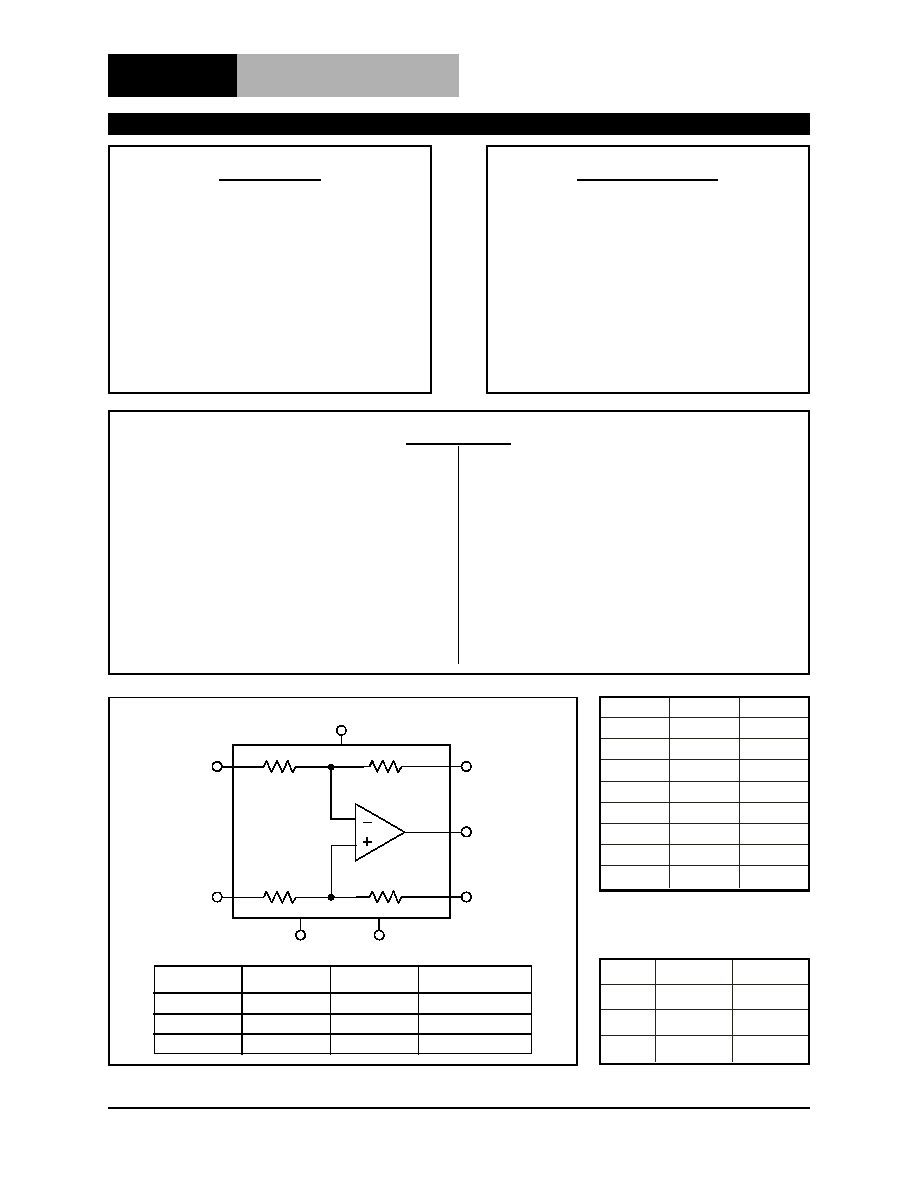
Sense
Vout
Ref
Vcc
Vee
In+
In-
NC
R
1
R
2
R
3
R
4
Gain
R , R
9 k
1
3
O
O
O
10.5 k
12 k
R , R
9 k
2
4
O
O
O
7.5 k
6 k
Part no.
THAT1240
THAT1243
THAT1246
0 dB
-3 dB
-6 dB
Fig ure 1. THAT1240-series equiva lent cir cuit dia gram
Gain
Plas tic DIP
Plas tic SO
0 dB
1240P08-U
1240S08-U
-3 dB
1243P08-U
1243S08-U
-6 dB
1246P08-U
1246S08-U
Ta ble 2. Or der ing infor ma tion
Pin Name
DIP Pin
SO Pin
Ref
1
1
In-
2
2
In+
3
3
Vee
4
4
Sense
5
5
Vout
6
6
Vcc
7
7
NC
8
8
Ta ble 1. 1240 Se ries pin assign ments
Bal anced Line Re ceiver ICs

THAT Corporation; 45 Sumner Street; Milford, Massachusetts 01757-1656; USA
Tel: +1 (508) 478-9200; Fax: +1 (508) 478-0990; Web: www.thatcorp.com
Page 2
THAT 1240 Se ries
Bal anced Line Re ceiver ICs
SPEC I FI CA TIONS
1
Ab so lute Max i mum Rat ings
Pos i tive Sup ply Volt age (V
CC
)
+20 V
Neg a tive Sup ply Volt age (V
EE
)
-20 V
Stor age Tem per a ture Range (T
ST
)
-40 to +125∞C
Out put Short-Circuit Du ra tion (t
SH
)
Con tin u ous
In put Volt ages (In+, In-)
±
50 V
Power Dis si pa tion (P
D
) (T
A
= 85∞C)
400 mW (DIP)
Power Dis si pa tion (P
D
) (T
A
= 85∞C)
260 mW (SO)
Op er ating Tem per a ture Range (T
OP
)
0 to 85∞C
Junc tion Tem per a ture (T
J
)
125∞C
Lead Tem per a ture (Sol dering 10 sec onds)
300 ∞C
Elec tri cal Char ac ter is tics
2
Pa ram e ter
Sym bol
Con di tions
Min
Typ
Max
Units
Sup ply Cur rent
I
CC
No sig nal
--
2.0
2.8
mA
Sup ply Volt age
V
CC
+3
+18
V
V
EE
-3
-18
V
In put Volt age Range
V
IN-DIFF
Dif fer en tial (equal and op po site swing)
THAT 1240 (0 dB gain)
--
21.5
--
dBu
3
THAT 1243 (-3 dB gain)
--
24.4
--
dBu
THAT 1246 (-6 dB gain)
--
27.5
--
dBu
V
IN-CM
Com mon mode
THAT 1240 (0 dB gain)
--
27.5
--
dBu
THAT 1243 (-3 dB gain)
--
29.1
--
dBu
THAT 1246 (-6 dB gain)
--
31.5
--
dBu
In put Im ped ance
4
Z
IN-CM
Com mon mode (all ver sions)
--
9
--
k
Z
IN-DIFF
Dif fer en tial
THAT 1240 (0 dB gain)
--
18
--
k
THAT 1243 (-3 dB gain)
--
21
--
k
THAT 1246 (-6 dB gain)
--
24
--
k
Com mon Mode Re jec tion Ra tio
CMRR
Matched source im ped ances; V
CM
= ±10 V
DC
70
90
--
dB
60 Hz
70
90
--
dB
20 kHz
70
85
--
dB
Power Sup ply Re jec tion Ra tio
5
PSR
at 60 Hz, with V
CC
= -V
EE
THAT 1240 (0 dB gain)
--
90
--
dB
THAT 1243 (-3 dB gain)
--
90
--
dB
THAT 1246 (-6 dB gain)
--
90
--
dB
To tal Har monic Dis tor tion
THD
V
IN-DIFF
= 10V; BW = 20 kHz;
f = 1 kHz, R
L
= 2 k
--
0.0006
--
%
Small Sig nal Band width
BW
-3dB
R
L
= 2 k
; C
L
= 10 pf
THAT 1240 (0 dB gain)
--
8.6
--
MHz
THAT 1243 (-3 dB gain)
--
12.2
--
MHz
THAT 1246 (-6 dB gain)
--
18
--
MHz
R
L
= 2 k
; C
L
= 300 pf
THAT 1240 (0 dB gain)
--
10.3
--
MHz
THAT 1243 (-3 dB gain)
--
11.8
--
MHz
THAT 1246 (-6 dB gain)
--
13.4
--
MHz

Doc u ment 600035 Rev 02
Page 3
THAT Corporation; 45 Sumner Street; Milford, Massachusetts 01757-1656; USA
Tel: +1 (508) 478-9200; Fax: +1 (508) 478-0990; Web: www.thatcorp.com
Out put Noise
e
(OUT)
22 Hz to 22 kHz band width
THAT 1240 (0 dB gain)
--
-103
--
dBu
THAT 1243 (-3 dB gain)
--
-105
--
dBu
THAT 1246 (-6 dB gain)
--
-106
--
dBu
Slew Rate
SR
R
L
= 2 k
; C
L
= 300 pf
7
12
--
V/
µ
s
Out put Gain Er ror
G
ER(OUT)
f = 1 kHz
-0.05
0
+0.05
dB
Out put Volt age Swing
V
O+
R
L
= 2 k
V
CC
- 2.5
V
CC
-2
--
V
V
O+
R
L
= 2 k
--
V
EE
+ 2 V
EE
+ 2.5
V
Out put Off set Volt age
V
OFF
No sig nal
-7
--
+7
mV
Out put Short Cir cuit Cur rent
I
SC
R
L
= 0
--
±25
--
mA
Re sis tive Load
R
L
2
--
--
k
Ca pac i tive Load
C
L
--
--
300
pF
Pack age Char ac ter is tics
Pa ram e ter
Sym bol
Con di tions
Min
Typ
Max
Units
Through-hole Pack age
Type
See Fig ure 14, Page 10 for di men sions
8-Pin PDIP
Ther mal Re sis tance
JA
DIP pack age sol dered to board
-
100
-
∫C/W
Sur face Mount Pack age
Type
See Fig ure 15, Page 10 for di men sions
8-Pin SOP
Ther mal Re sis tance
JA
SO pack age sol dered to board
-
150
-
∫C/W
Sol dering Reflow Pro file
JEDEC JESD22-A113-B (220 ∫C)
1
All spec i fi ca tions are sub ject to change with out no tice.
2
Un less oth er wise noted, T
A
=25∞C, V
CC
= +15V, V
EE
= -15V, Test cir cuit is as shown in Fig ure 2.
3
0 dBu = 0.775Vrms.
4
While spe cific re sis tor ra tios are very closely trimmed, ab so lute re sis tance val ues can vary ±25% from the
typ i cal val ues shown. In put im ped ance is mon i tored by lot sam pling.
5
De fined with re spect to dif fer en tial gain.
The ory of Op er a tion
The THAT1240-series ICs con sist of high per for -
mance opamps with in te grated, la ser-trimmed re sis -
tors. These de signs take full ad van tage of THAT's
fully com ple men tary di elec tric iso la tion (DI) pro cess
to de liver ex cel lent per for mance with low cur rent
con sump tion. The de vices are sim ple to ap ply in
many ap pli ca tions.
Re sis tor Trimming, Values, and CMRR
The 1240-series de vices rely upon pro pri etary,
la ser-trimmed, sil i con-chromium (Si-Cr), thin-film,
in te grated re sis tors to de liver the pre cise match ing
re quired to achieve a 90dB com mon mode re jec tion
ra tio. Trimming is per formed in two cy cles, both us -
ing dc in puts. First, gain is set by trim ming the
R
1
/R
2
pair. Then, CMRR is set by trim ming the other
pair (R
3
/R
4
). Gen erally, only one re sis tor of each pair
is trimmed (which ever needs to in crease to meet the
re quired spec i fi ca tion).
To achieve 90 dB CMRR, the R
3
/R
4
ra tio is
trimmed to within ±0.005 % of the R
1
/R
2
ra tio.
Since the re sis tors them selves are on the or der of
10 k
(see Fig ure 1 for ac tual val ues, which change
with the spe cific part), an in crease of as lit tle as
0.6
can re duce the CMRR from over 90 dB to only
84 dB. The better the start ing CMRR, the more im -
pact (in dB) a given added re sis tance will have.
There fore, to achieve this high CMRR in prac tice,
care should be taken to en sure that all source im -
ped ances re main bal anced. To ac com plish this,
PCB traces car ry ing sig nal should be bal anced in
length, con nec tor re sis tance should be min i mized,
and any in put ca pac i tance (in clud ing strays) should
be bal anced be tween the + and - legs of the in put
cir cuitry. Note that the ad di tional con tact re sis tance
of some sock ets is suf fi cient to undo the ef fects of
pre ci sion trim ming. There fore, sock et ing the parts
is not rec om mended. THAT's 1200-series InGenius
Æ
in put stages ad dress many of these dif fi cul ties
through a pat ented method of in creas ing com -
mon-mode in put im ped ance.
A fur ther con sid er ation is that af ter trim ming,
the two re sis tor di vider ra tios are tightly con trolled,
but the ac tual value of any in di vid ual re sis tor is not.
In fact, two of the four re sis tors are nor mally left
with out trim ming. The ini tial tol er ance of the re sis -
tors is quite wide, so it is pos si ble for any given re -
sis tor to vary over a sur pris ingly wide range,
Lot-to-lot vari a tions of up to ±25 % are to be ex -
pected.
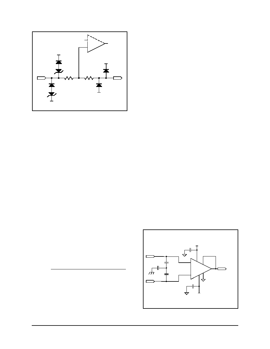
In put Con sid er ations
The 1240-series de vices are in ter nally pro tected
against in put over load via an un usual ar range ment
of di odes con nect ing the + and - In put pins to the
power sup ply pins. The cir cuit of Fig ure 3 shows the
ar range ment used for the R
3
/ R
4
side; a sim i lar one
ap plies to the other side. The zener di odes pre vent
the pro tec tion net work from con duct ing un til an in -
put pin is raised at least 50 V above V
CC
or be low
V
EE
. Thus, the pro tec tion net works pro tect the de -
vices with out con strain ing the al low able sig nal swing
at the in put pins. The ref er ence (and sense) pins are
THAT Corporation; 45 Sumner Street; Milford, Massachusetts 01757-1656; USA
Tel: +1 (508) 478-9200; Fax: +1 (508) 478-0990; Web: www.thatcorp.com
Page 4
THAT 1240 Se ries
Bal anced Line Re ceiver ICs
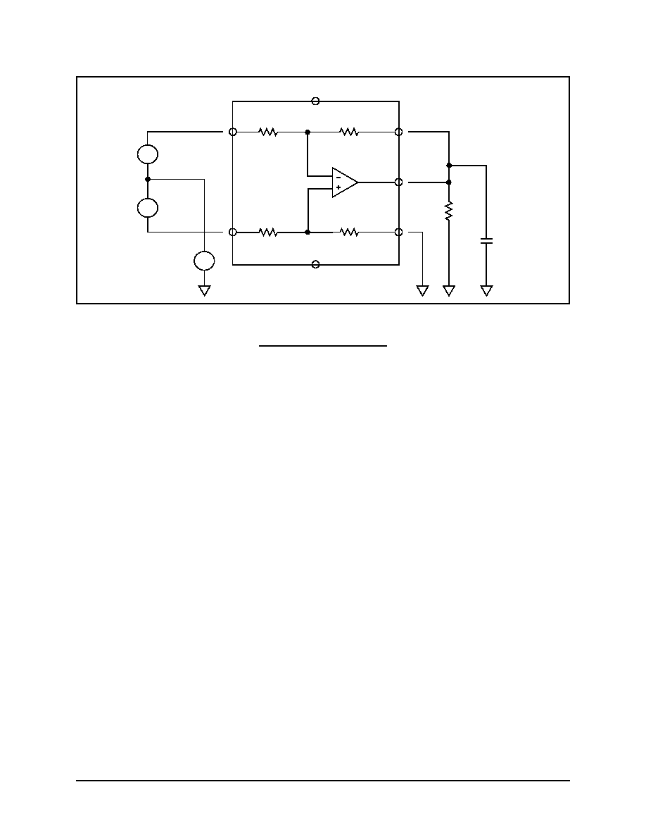
R
2
R
1
R
4
R
3
Sense
Vout
Ref
V
CC
V
EE
V
IN(CM)
In+
In-
R
L
Ωv
IN(DIFF)
~
~
~
b
a
C
L
Ωv
IN(DIFF)
Fig ure 2. THAT1240 se ries test cir cuit
pro tected via more con ven tional re verse-biased di -
odes which will con duct if these pins are raised
above V
CC
or be low V
EE
.
Be cause the 1240-series de vices are in put stages,
their in put pins are of ne ces sity con nected to the
out side world. This is likely to ex pose the parts to
ESD when ca bles are con nected and dis con nected.
Our test ing in di cates that the 1240-series de vices
will typ i cally with stand ap pli ca tion of up to 1,000
volts un der the hu man body ESD model.
To re duce risk of dam age from ESD, and to pre -
vent RF from reach ing the de vices, THAT rec om -
mends the cir cuit of Fig ure 4. C
3
through C
5
should
be lo cated close to the point where the in put sig nal
co mes into the chas sis, pref er a bly di rectly on the
con nec tor. The un usual cir cuit de sign is in tended to
min i mize the un bal anc ing im pact of dif fer ences in
the val ues of C
4
and C
5
by forc ing the ca pac i tance
from each in put to chas sis ground to de pend pri -
mar ily on the value of C
3
. The cir cuit shown is ap -
prox i mately ten times less sen si tive to mis matches
be tween C
4
and C
5
than the more con ven tional ap -
proach, in which the junc tion of C
4
and C
5
is
grounded di rectly. An ex cel lent dis cus sion of in put
stage ground ing can be found in the June 1995 is -
sue of the Jour nal of the Au dio En gi neering So ci ety,
Vol. 43, No. 6, in ar ti cles by Ste phen Macatee, Bill
Whitlock, and oth ers.
Note that, be cause of the tight match ing of the in -
ter nal re sis tor ra tios, cou pled with the un cer tainty
in ab so lute value of any in di vid ual re sis tor, RF by -
pass ing through the ad di tion of R-C net works at the
in puts (se ries re sis tor fol lowed by a ca pac i tor to
ground at each in put) is not rec om mended. The
added re sis tors can in ter act with the in ter nal ones
in un ex pected ways. If some im ped ance for the
RF-bypass ca pac i tor to work against is deemed nec -
es sary, THAT rec om mends the use of a fer rite bead
or balun in stead.
If it is nec es sary to ac-couple the in puts of the
1240-series parts, the cou pling ca pac i tors should be
sized to pres ent neg li gi ble im ped ance at any fre -
quen cies of in ter est for com mon mode re jec tion. Re -
gard less of the type of cou pling ca pac i tor cho sen,
vari a tions in the val ues of the two ca pac i tors, work -
ing against the 1240-series in put im ped ance (it self
sub ject to po ten tial im bal ances in ab so lute value,
even when trimmed for per fect ra tio match), can un -
bal ance com mon mode in put sig nals, con vert ing
them to bal anced sig nals which will not be re jected
by the CMRR of the de vices. For this rea son, THAT
rec om mends dc-coupling the in puts of the
1240-series de vices.
In put Volt age Lim i ta tions
When con fig ured, re spec tively, for -3 dB and
-6 dB gain, the 1243 and 1246 de vices are ca pa ble
of ac cept ing in put sig nals above the power sup ply
rails. This is be cause the in ter nal opamp's in puts
con nect to the out side world only through the
on-chip re sis tors R
1
through R
4
at nodes a and b as
shown in Fig ure 2. Con sider the fol low ing anal y sis.
Dif fer en tial In put Sig nals
For dif fer en tial sig nals (v
IN(DIFF)
), the lim i ta tion to
sig nal han dling will be out put clip ping. The out puts
of all the de vices typ i cally clip at within 2V of the
sup ply rails. There fore, max i mum dif fer en tial in put
sig nal lev els are di rectly re lated to the gain and sup -
ply rails.
THAT Corporation; 45 Sumner Street; Milford, Massachusetts 01757-1656; USA
Tel: +1 (508) 478-9200; Fax: +1 (508) 478-0990; Web: www.thatcorp.com
Doc u ment 600035 Rev 02
Page 5
-
+
In+
Ref
V
CC
V
EE
V
CC
V
EE
R
3
R
4
Fig ure 3. Rep re sen ta tive In put Pro tec tion Circuit
C4
470p
C5
470p
C3
47p
In+
In-
Out
C1
100n
C2
100n
V
CC
V
EE
In-
2
In+
3
Out
6
U1
THAT1246/1243/1240
Ref
Sens
V
EE
V
CC
5
7
4
1
Fig ure 4. RFI and Sup ply Bypassing